DMX Shield for Arduino with isolation
This DMX Shield enables sending and receiving DMX signals by using a save DMX hardware including isolation. Ideal for DMX projects without risking processor damages from high voltage peaks.
I had published some previous versions here. This is the newest version of the shield that has no additional functions and works exactly like the shield in version v03 that is in use in multiple installations. But there are some improvements by adjusting some values and make its use more flexible when using it on top of an Arduino MEGA and other shields.
Download
Download the project files including the Eagle based schema and board design: DMXShield.zip (Version 7)
I sometimes may have some boards available so you can ask for per mail.
Hardware design of the shield
The ideas behind the hardware design are:
-
One shield for DMX sending and receiving
There are some Arduino Shield designs and standalone projects available that only support for one direction of communication. Because I played around with both scenarios I built a solution that allows both roles in a DMX setup. When only a receiver or sender situation is needed it is possible to leave some components unpopulated. -
Support of DMX and RDM
This requirement results in an explicit controlling of the direction of the communication and enabling/disabling the receiving and sending drivers. Also the main controller also has to be terminated and must provide a bias to keep the level in the ‘marking state’ when no driver is enabled. -
Galvanic decoupling
If you like a robust system and like to use your laptop or computer in a rough environment it is essential to decouple the systems and eliminate so called ground loops. Especially on stage you’ll be glad about that! -
Simple solution for beginners
All the components can be mounted on the Shield without much soldering experience and the extra components for supporting RDM and extra components for isolation can easily be left away - The shield also provides 3 PWM LED outputs (red, green and blue).
- The DMX sockets are not part of the Shield layout to enable a flexible design of the box.
Schema
The schema for this board is designed to use the standard serial interface of the Arduino board for sending and receiving DMX data packages. Therefore the pin 0 and 1 are used to read and send the data. To switch the data direction between sending and receiving the digital pin 2 is used.
Here is the complete layout (click to enlarge):

(click to open a full size picture).
The details of the shield design are discussed below.
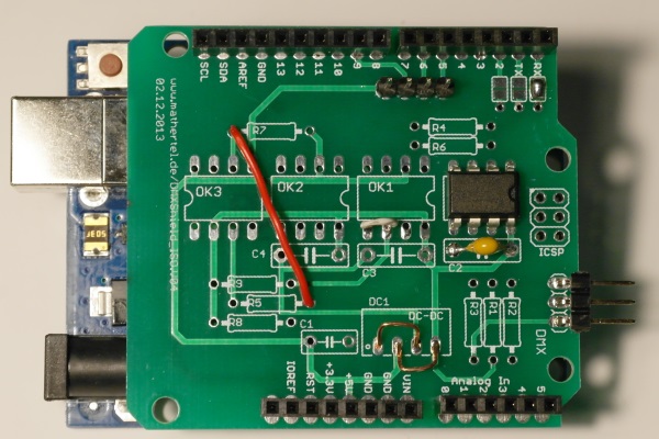
Here is a picture of a fully assembled shield on top of an Arduino UNO:

(click to open a full size picture).
Driver Chips and DMX bus termination
When searching the internet you can see several chips being used to drive a DMX communication. They all are made to convert logic-level signals (LOW & HIGH) to the EIA-485 differential signal levels on the twisted pair cable.
Very common are the chips from MAXIM that I also use for my implementation. The one I prefer is the MAX485 or MAX481 which are identical with the exception of a low power shut down mode in MAX481 that we don’t need in the DMX scenario. MAX481 and MAX485 from MAXIM: http://www.maxim-ic.com/datasheet/index.mvp/id/1111
Other chips often used are the 75176b differential bus transceivers from Texas Instruments.
A typical schema using MAX481 for a DMX controller is:

In addition a +5V supply must be connected to pin 8 and the ground level to pin 5 of the MAX481 chip.
The three resistors are the termination of the DMX bus. These resistors MUST be present at the controlling node of a DMX bus. R2 is eliminating echo packets while R1 and R3 keep the DMX line in logical HIGH state when no controller is sending. This is especially useful when implementing RDM supporting controllers.
A controller that is not designed for RDM can leave the resistors R1 and R3 un-assembled and use a R2 resistor with 120 Ω.
When using the DMX controller chip within a slave node the resistors on the board SHOULD NOT be populated at all. The last node of the DMX bus MUST be terminated using a termination socket with a 120 Ω inside.
The pin 2 of that chip controls whether the receive (pin 1) is active and pin 3 does the same for the output direction (pin 4). Because the pin 2 is internally inverted (marked as an invertion sign at pins 2 connection to the amplifier) both pins can connected together and can be controlled only by one logical signal. If the signal is high the output direction is enabled, if the signal is low, the input direction is enabled.
Isolation
For a simple setup it is possible to connect the Driver chip directly to the Arduino pins but if you need a robust system, especially on a stage environment, you will have to add some more electronics to avoid electrical damage by defect equipment or accidental circumstances.
The electric potential of the DMX side of the implementation have to be isolated from the processor. There are 2 sort of chips that implement all you need:
-
A 5 volt to 5 volt DC/DC converter with galvanic decoupling.
There are complete solutions in a single component available like NME0505SC or AM1S-0505SZ that can be used to generate a 5V power supply that is galvanic isolated up to 1000V. So even if there is a high voltage attached to the DMX bus there is a chance of no or low damage. -
High speed TTL compatible Optocouplers
These chips use a LED and light sensitive transistor to isolate the DMX bus from the Arduino data pins. There are standard TTL compatible Optocouplers available like the 6N137 from MOTOROLA.
There are 3 data signals from the arduino that have to be brought from the arduino side to the DMX side: transmit, receive and the data direction:

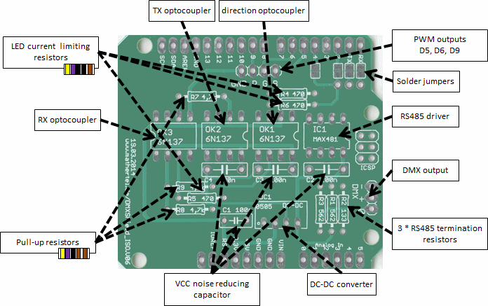
Full partslist & building plan
| Part name | Value | Description |
|---|---|---|
| Starting with the low parts... | ||
| R4, R5, R6 | 470 Ω | Bands: (yellow, purple, black, black, brown*) or (yellow, purple, brown, silver*) |
| R7, R8, R9 | 4,7 kΩ | Bands: (yellow, purple, black, brown, brown*) or (yellow, purple, red, silver*) |
|
The resistors R1 - R3 should be adjusted for the
role of the DMX board in your DMX setup. This configuration is for a DMX / RDM Controller. Don't use them when implementing a DMX or RDM Slave. |
||
| R1, R3 | 562 Ω | Bands: (green, blue, red, black, brown*) |
| R2 | 133 Ω | Bands: (brown, orange, orange, black, brown*) |
| Now the capacitors... | ||
| C1,C2,C3,C4 | 100n | Capacitors stabilizing the power. Label: 104 |
| The dc-dc converter... | ||
| DC1 | NME 0505 | A dc-dc-converter. The chip that provides another 5 v source for the DMX signal converter. |
| Now you can check if the secondary 5v power is existing. Put it on top of an Arduino and measure the voltage at the capacitor C4. It should be near by 5V. | ||
| The optocouplers and the driver chips... | ||
| IC1 | MAX481CPA |
A MAX481CPA or MAX485 CPA from Maxim or another supplier used to
convert the differential DMX signal into a logical signal. The 8 pin chip can be soldered directly or put on a socket. Be sure to place it in the right direction. |
| OK1, OK2, OK3 | 6N137 |
The optocouplers. The 8 pin chip can be soldered directly or put on a socket. Be sure to place it in the right direction. |
| ...and the connectors | ||
| DMX | 1X03 pinhead. I cut it from a longer (20 pin) one. | |
| RGB | 1X04 pinhead | |
| stackable headers | You can solder the usual stackable headers or if you use the shield at the uppermost shield on the Arduino you can solder simple pinheads too. | |
| ICSP | There is no need caused by this shield to solder a ICSP. You can solder one if you like to use the shield with another shield above that needs these connections. | |
| solder jumpers | Don’t forget to close the jumpers when using a standard Arduino. | |
And here is a picture that shows where the parts are located on the board:
Simplifying opportunities
When equipping the board it is possible to let off some components and thus to achieve simplification and cost reduction.
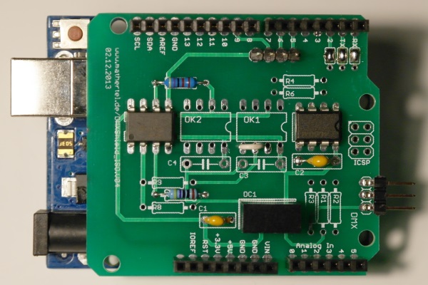
No Isolation, DMX Device only
Here is a picture of a partly assembled shield where all isolating components have been left off and only the sending and direction signal have been bridged:
You can see that only RX solder jumper is closed, the DC-DC converter and the pins 5 and 6 at OK1 are bridged.
No Isolation, full RDM compatible
Here is a picture of a partly assembled shield where all isolating components have been left off but all functions are enabled (send receive and direction switch:
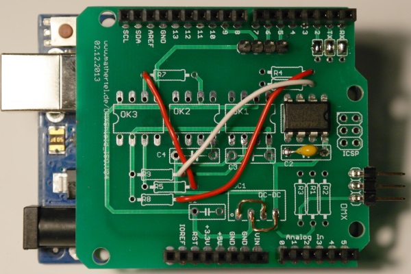
All solder jumper are closed, the DC-DC converter is bridged and the wires skip the optocouplers.
DMX Device with isolation with that can only receive data
Here is a picture of a partly assembled shield where only the rx is transferred by using OK3.
I have included some comments in the parts list for using the board as a DMX Master, RDM Master and DMX/RDM Slave.
If you only need a DMX Master or DMX slave configuration the data direction can be set to a constant level.
If you only need to send then you should not connect the RX signal so you can still use the USB to upload sketches.
Some details on the shield layout
Flexibility for Arduino MEGA
The signals RX, TX and D2 are now brought to the pins d0, d1, d2 via a solder jumper. These 3 jumpers should be closed by dropping a small part of solder upon them for normal operation with Arduino Uno or Leonardo Boards.
If you like to use other serial ports or signals like on the Arduino MEGA you can leave these jumpers open and connect the signals the way you like.
The ICSP header of the Arduino board can now be brought to the next shield above the DMX shield by soldering a stackable header.
All the 4 holes from the Arduino Uno Board are now also available to the shield for building permanent robust stacks.
ICSP header and more pins
All of these extensions are not needed by the DMX shield but it is a good practice to have connection pads and holes at these positions so the signals can be passed through.
Some Arduino shields are using the ICSP header to access the SPI signals from the ATmega chip. The Ethernet shield is a good example for that and there are good reasons to do so.
Not the new version of the DMX shield has 6 contacts right where a ICSP connector can be soldered to pass through the signals to a shield above.
Also 2 of the Arduino header pins have been expanded since some versions. The POWER connector is now 8 pins long and includes IOREF signal. The upper digital connector is now 10 pins long and include the SDA and SCL signals.
Because the DMX shield does not need these signals you can leave these pins without soldering a header or use the (old) shorter headers if you like.
Solder Jumpers
The solder jumpers on Arduino DMX Shield are there to have flexibility in the case of Arduino Mega and Arduino Leonard boards.
For the Uno and older boards with the ATmega328 or ATmega168 processor you just have to close the jumpers near the pins 0, 1 and 2. But there are some options available you might consider.
Using the RX/TX jumpers
Closing the jumpers at the pins 0 (RX) and 1 (TX) will enable the standard serial port to be used for sending and receiving the DMX data and pin 2 is used for switching the send/receive data direction. This is the default signal layout I used for the last years and it's recommended for UNO boards.
If you like to use another serial port you just can leave the solder jumpers open and connect to the other pins by using small cables. The small holes nearby the jumpers are there for attaching them.
The connections at pin 0 and 1 have to be connected to any other serial interface.
I/O direction and pin conflicts
The connection near pin 2 has to be connected to a digital signal for switching the send/receive data direction and using pin 2 is the standard option. You need a HIGH signal for sending and a LOW signal for receiving.
This is automatically done by the DMXSerial library according to the operation mode passed to the init() function. The DMXSerial2 library that implements RDM normally listens to DMX signal but when requested to send a packet back to the controller this library switches the level of the pin as needed.
On the Leonardo board with the ATmega32u4 processor the digital pin 2 is in conflict to the SDA signal of the I2C bus hardware. If you like to use both interfaces at once you have to use another port for switching the send/receive data direction.
Therefore, starting with revision 6 of this board another solder jumper is available at pin 4 and you should close the solder jumper at pin 4 and not at pin 2 and give the pin 4 to the init() function of DMXSerial or DMXSerial2 library.
Links
A schema design I used for designing this shield can be found at: http://www.mikrocontroller.net/topic/190608.
ChangeLog
- 02.09.2011 Published PCB version v02.
- 22.11.2012 Version v03 including a new connector for simple RGB LED.
- 10.01.2013 It's proofed: The shield is also working with RDM packets.
- 07.04.2014 Version 4 of the shield with improved layout and solder jumpers.
- 19.03.2015 Version 6 of the shield with solder jumpers for enabling pin 4 for data direction.
- Version 7 comes only with some cleanup and labels nearby pins.